|
| |
|
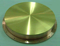
Physical vapor deposition (PVD) describes a variety of vacuum deposition methods used to deposit thin film by the condensation of a vaporized form of the desired film material onto various workpiece surfaces (e.g., onto semiconductor walfers).
Sputtering target source is bombarded by a glow plasma discharge with argon ions(usually localized around the "target" by a magnet), and a uniform metal film is coated on the workpiece surfaces.
Those products are widely used for the semiconductor and electronic industry, for example, data storage media, laser memory, IC(integrated circuit), LCD( liquid crystal display), control component, advanced contact materials, wear resistant materials, corrosion resistant materials, large area glass coatings and so on.
|
|
 |
 |
|
Materials of Sputtering Targets |
| |
Au, Au-Ag alloys, Au-Ni alloys and other gold alloys;
|
Ag, Ag-Cu alloys and othe silver allys;
|
Pt, Pt-Ni allys and other
platinum
alloys;
|
Pd, Pd-Ag alloys and other
palladium
alloys;
|
Ti, Ni, Si, W, Mo;
|
Ta2O5, Nb2O5, SrTiO3, BaTiO3, SnO2+Pt(Pd).
|
|
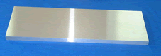
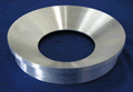
Note: We can supply sputtering targets for customized shape, dimensions and purity.
|
|
|

.gif)